Research Brief: Altium Develop gives your entire electronics team real-time visibility into Multidisciplinary product creation powered by your unconstrained network.
Signal Ground Power Ground 4 Layer Stackup Pcb Design Explained - General Main Notes
This guide collects Signal Ground Power Ground 4 Layer Stackup Pcb Design Explained with background information, practical notes, and nearby searches before opening more specific references.
In addition, this page also connects Signal Ground Power Ground 4 Layer Stackup Pcb Design Explained with for broader topic coverage.
General Main Notes
Multidisciplinary product creation powered by your unconstrained network. Altium Develop gives your entire electronics team real-time visibility into
Topic Details to Compare
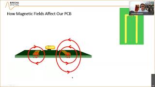
Ali Shirsavar - Biricha Digital Fundamentals of noise coupling in electronic circuits are surprisingly straight forward if we ...
Follow-Up Ideas for Readers
Use the related entries as follow-up paths when you need more examples, current details, or alternative wording.
Practical Meaning
This part keeps Signal Ground Power Ground 4 Layer Stackup Pcb Design Explained connected to practical references instead of leaving it as a single isolated phrase.
Quick reference points
- Multidisciplinary product creation powered by your unconstrained network.
- Altium Develop gives your entire electronics team real-time visibility into
- Ali Shirsavar - Biricha Digital Fundamentals of noise coupling in electronic circuits are surprisingly straight forward if we ...
What this page helps clarify
This format works because it offers follow-up questions for Signal Ground Power Ground 4 Layer Stackup Pcb Design Explained before checking official or primary sources.
Useful FAQ
How does Signal Ground Power Ground 4 Layer Stackup Pcb Design Explained connect to reference?
Signal Ground Power Ground 4 Layer Stackup Pcb Design Explained can connect to reference when readers need context, examples, comparisons, or practical next steps inside the same topic area.
How does Signal Ground Power Ground 4 Layer Stackup Pcb Design Explained connect to resource?
Signal Ground Power Ground 4 Layer Stackup Pcb Design Explained can connect to resource when readers need context, examples, comparisons, or practical next steps inside the same topic area.
What should be avoided when researching Signal Ground Power Ground 4 Layer Stackup Pcb Design Explained?
Avoid treating one short snippet as complete, especially when the topic involves money, health, law, schedules, or current details.