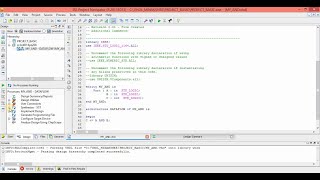
Topic Snapshot: A logical OR operation has a high output (1) if one or both the inputs to the Design and Simulation all the logic gates using VHDL on Xilinx ISE Design Suite

Xilinx Ise Design Suite 14 7 Simulation Tutorial Vhdl Code For And Gate - General Common Use Cases

Use this page to review Xilinx Ise Design Suite 14 7 Simulation Tutorial Vhdl Code For And Gate with main details, supporting notes, and connected entries so readers can continue exploring with more context.

In addition, this page also connects Xilinx Ise Design Suite 14 7 Simulation Tutorial Vhdl Code For And Gate with for broader topic coverage.

General Common Use Cases

Design and Simulation all the logic gates using VHDL on Xilinx ISE Design Suite A logical OR operation has a high output (1) if one or both the inputs to the

General Next Search Paths

Use the related entries as follow-up paths when you need more examples, current details, or alternative wording.

General Guide

This section introduces Xilinx Ise Design Suite 14 7 Simulation Tutorial Vhdl Code For And Gate with the most useful background points and a simple path into the rest of the page.

Topic Practical Details

The key details usually include definitions, examples, comparisons, requirements, limitations, and updated references.

Important details found

  • Design and Simulation all the logic gates using VHDL on Xilinx ISE Design Suite
  • A logical OR operation has a high output (1) if one or both the inputs to the

How readers can use this page

Readers often search for Xilinx Ise Design Suite 14 7 Simulation Tutorial Vhdl Code For And Gate because they want better wording, relevant follow-ups, and useful checks.

Sponsored

Common Questions

What related areas connect to Xilinx Ise Design Suite 14 7 Simulation Tutorial Vhdl Code For And Gate?

Related areas may include comparisons, examples, requirements, common mistakes, updated references, and practical follow-up guides.

How does Xilinx Ise Design Suite 14 7 Simulation Tutorial Vhdl Code For And Gate connect to guide?

Xilinx Ise Design Suite 14 7 Simulation Tutorial Vhdl Code For And Gate can connect to guide when readers need context, examples, comparisons, or practical next steps inside the same topic area.

Why might Xilinx Ise Design Suite 14 7 Simulation Tutorial Vhdl Code For And Gate have several meanings?

Different pages may focus on different locations, dates, providers, versions, definitions, or user needs.

How can related pages improve understanding of Xilinx Ise Design Suite 14 7 Simulation Tutorial Vhdl Code For And Gate?

Related pages add context, alternative wording, practical examples, and follow-up paths for deeper research.

Supporting Media Notes

Xilinx ISE Design Suite 14.7 Simulation Tutorial || VHDL Code for  AND Gate
And Gate in Xilinx | Xilinx Tutorial
Xilinx ISE: Design and simulate VERILOG HDL Code
Full Adder Verilog Code in Data Flow Modelling / xilinx 14.7
OR Gate in Xilinx using VHDL Code Simulation
Design and Simulation all the logic gates using VHDL on Xilinx ISE Design Suite
Or Gate in Xilinx | Xilinx Tutorial
Design simple combitional logic circuit using VHDL  Using Xilinx ISE Simulator
AND Gate using VHDL and ISE Design Suite Xilinx.
AND gate simulation in ISE Design Suite 14.2 using VHDL Code
Sponsored
Continue Reading
Xilinx ISE Design Suite 14.7 Simulation Tutorial || VHDL Code for  AND Gate

Xilinx ISE Design Suite 14.7 Simulation Tutorial || VHDL Code for AND Gate

Read more details and related context about Xilinx ISE Design Suite 14.7 Simulation Tutorial || VHDL Code for AND Gate.

And Gate in Xilinx | Xilinx Tutorial

And Gate in Xilinx | Xilinx Tutorial

Read more details and related context about And Gate in Xilinx | Xilinx Tutorial.

Xilinx ISE: Design and simulate VERILOG HDL Code

Xilinx ISE: Design and simulate VERILOG HDL Code

Read more details and related context about Xilinx ISE: Design and simulate VERILOG HDL Code.

Full Adder Verilog Code in Data Flow Modelling / xilinx 14.7

Full Adder Verilog Code in Data Flow Modelling / xilinx 14.7

Read more details and related context about Full Adder Verilog Code in Data Flow Modelling / xilinx 14.7.

OR Gate in Xilinx using VHDL Code Simulation

OR Gate in Xilinx using VHDL Code Simulation

A logical OR operation has a high output (1) if one or both the inputs to the

Design and Simulation all the logic gates using VHDL on Xilinx ISE Design Suite

Design and Simulation all the logic gates using VHDL on Xilinx ISE Design Suite

Design and Simulation all the logic gates using VHDL on Xilinx ISE Design Suite

Or Gate in Xilinx | Xilinx Tutorial

Or Gate in Xilinx | Xilinx Tutorial

Read more details and related context about Or Gate in Xilinx | Xilinx Tutorial.

Design simple combitional logic circuit using VHDL  Using Xilinx ISE Simulator

Design simple combitional logic circuit using VHDL Using Xilinx ISE Simulator

Read more details and related context about Design simple combitional logic circuit using VHDL Using Xilinx ISE Simulator.

AND Gate using VHDL and ISE Design Suite Xilinx.

AND Gate using VHDL and ISE Design Suite Xilinx.

Read more details and related context about AND Gate using VHDL and ISE Design Suite Xilinx..

AND gate simulation in ISE Design Suite 14.2 using VHDL Code

AND gate simulation in ISE Design Suite 14.2 using VHDL Code

Read more details and related context about AND gate simulation in ISE Design Suite 14.2 using VHDL Code.