Topic Notes: Multidisciplinary product creation powered by your unconstrained network.

Introduction Of A 4 Layer Pcb With Countersink Holes - General What to Confirm

Use this page to review Introduction Of A 4 Layer Pcb With Countersink Holes with main details, supporting notes, and connected entries without jumping between unrelated pages.

In addition, this page also connects Introduction Of A 4 Layer Pcb With Countersink Holes with for broader topic coverage.

General What to Confirm

Important details can vary by source, so this page groups the most readable points into a scannable format.

Topic Important Context

This part keeps Introduction Of A 4 Layer Pcb With Countersink Holes connected to practical references instead of leaving it as a single isolated phrase.

Key Overview for Readers

Introduction Of A 4 Layer Pcb With Countersink Holes can be reviewed through a clear overview first, then compared with related entries and supporting context.

Reference Review Notes

Use the related entries as follow-up paths when you need more examples, current details, or alternative wording.

Relevant points collected here

  • Multidisciplinary product creation powered by your unconstrained network.

How this reference can help

A structured page helps readers move from a simple way to compare connected search results.

Sponsored

Questions People Also Check

Why might Introduction Of A 4 Layer Pcb With Countersink Holes have several meanings?

Different pages may focus on different locations, dates, providers, versions, definitions, or user needs.

How can related pages improve understanding of Introduction Of A 4 Layer Pcb With Countersink Holes?

Related pages add context, alternative wording, practical examples, and follow-up paths for deeper research.

How can readers make Introduction Of A 4 Layer Pcb With Countersink Holes more specific?

Different pages may focus on different locations, dates, providers, versions, definitions, or user needs.

Why do people search for Introduction Of A 4 Layer Pcb With Countersink Holes?

People often search for Introduction Of A 4 Layer Pcb With Countersink Holes to understand the basics, compare related options, or find a clearer path to more specific information.
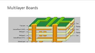
Image-Based Context

Introduction of a 4-layer PCB with countersink holes
Designing a 4 Layer PCB Stackup With 50 Ohm Impedance | Signal Integrity
Signal Ground Power Ground 4-Layer Stackup? PCB Design Explained!
PCB Layer Stackup basics for Beginners: A Simple Guide | 4 Layer PCB Stackup in 2025 |
How To Define a 4 Layer PCB Stackup
[PCB] PCB 4Layer Process
Introduction to Basic Concepts in PCB Design
4 Layer PCB Power and Ground Plane Design Current Path and Density Considerations  #73
Two-Layer PCB Design Tips: Achieving the Optimal Layout
How to Design a 6-Layer PCB Stackup for Best Performance  #jlcpcb #pcbdesign #stackup
Sponsored
Browse Topic
Introduction of a 4-layer PCB with countersink holes

Introduction of a 4-layer PCB with countersink holes

Read more details and related context about Introduction of a 4-layer PCB with countersink holes.

Designing a 4 Layer PCB Stackup With 50 Ohm Impedance | Signal Integrity

Designing a 4 Layer PCB Stackup With 50 Ohm Impedance | Signal Integrity

Read more details and related context about Designing a 4 Layer PCB Stackup With 50 Ohm Impedance | Signal Integrity.

Signal Ground Power Ground 4-Layer Stackup? PCB Design Explained!

Signal Ground Power Ground 4-Layer Stackup? PCB Design Explained!

Multidisciplinary product creation powered by your unconstrained network. Work concurrently across design, sourcing, and ...

PCB Layer Stackup basics for Beginners: A Simple Guide | 4 Layer PCB Stackup in 2025 |

PCB Layer Stackup basics for Beginners: A Simple Guide | 4 Layer PCB Stackup in 2025 |

Read more details and related context about PCB Layer Stackup basics for Beginners: A Simple Guide | 4 Layer PCB Stackup in 2025 |.

How To Define a 4 Layer PCB Stackup

How To Define a 4 Layer PCB Stackup

Read more details and related context about How To Define a 4 Layer PCB Stackup.

[PCB] PCB 4Layer Process

[PCB] PCB 4Layer Process

Read more details and related context about [PCB] PCB 4Layer Process.

Introduction to Basic Concepts in PCB Design

Introduction to Basic Concepts in PCB Design

Read more details and related context about Introduction to Basic Concepts in PCB Design.

4 Layer PCB Power and Ground Plane Design Current Path and Density Considerations  #73

4 Layer PCB Power and Ground Plane Design Current Path and Density Considerations #73

Read more details and related context about 4 Layer PCB Power and Ground Plane Design Current Path and Density Considerations #73.

Two-Layer PCB Design Tips: Achieving the Optimal Layout

Two-Layer PCB Design Tips: Achieving the Optimal Layout

Multidisciplinary product creation powered by your unconstrained network. Work concurrently across design, sourcing, and ...

How to Design a 6-Layer PCB Stackup for Best Performance  #jlcpcb #pcbdesign #stackup

How to Design a 6-Layer PCB Stackup for Best Performance #jlcpcb #pcbdesign #stackup

Read more details and related context about How to Design a 6-Layer PCB Stackup for Best Performance #jlcpcb #pcbdesign #stackup.